The World's Most Expensive Bottleneck
ASML and the Unease of Having No Substitute
Earlier this year, I spoke with a VP at Morgan Stanley, an incredibly astute person. During our conversation, ASML was brought up and we went back and forth discussing how its moat is strong and risky. He then asked me a question "why would the world need more than one company?". His point was fair. Having a single trusted player at the centre of the global tech supply chain is, in fact, quite economically efficient. While my own view was tilted towards the risks of a bottleneck on society, I understood his rationale.
Recently, at UC Berkeley, I was exposed to the importance of semiconductors in multiple settings. So, I decided to go back to answering that question that was still unclear to me. Would the world benefit more from creating an alternative to ASML or from making the existing semiconductor ecosystem more resilient?
My answer is that ASML is very difficult to replicate. We pay for it through the cost that trickles down to users and we would pay far more if the supply chain broke.
Why is ASML so difficult to replicate
Semiconductors are today's digital oil and one of the most profitable sectors. Within this supply chain, ASML supplies the picks and shovels in today's AI gold rush and Elon Musk has called it "arguably the greatest company in Europe". The moat keeps widening and barriers to entry keep rising because of three reasons.
R&D & Technology
EUV lithography is the most complex system to ever be built, with more than 100,000 parts (more complex than particle accelerators or the International Space Station). A single High NA EUV costs $400 million, and ASML has no commercial rival in that category.
It has not always been this way. ASML began as an oligopoly alongside Nikon and Canon. It's edge came from the TWINSCAN breakthrough which increased throughput and decreased the cost per good yield, the two metrics chipmakers care about most. The breakthrough started a flywheel effect of R&D investment that widened the moat. ASML offered their customers to co-invest in the R&D of the next generation technology which helped to offset the any innovation investment risks. Since then, billions has been invested over three decades. For aspiring competitors, attempting to catch up implies investing billions as a sunk cost for decades with no guarantee of commercial viability. By that time, ASML would have already moved on to commercialising the next generation.
The engineers have an accumulation of the tacit knowledge and internalised expertise over the years lies within their brains and not in documents or software.
Upstream Supply Chain Lock In
ASML acts as a system integrator and manufactures only 15% of the machine itself. It has around 5,100 global suppliers who are specialised in their own right. Their key suppliers include Carl Zeiss which builds the optical systems used in the lithography machines, TRUMPF supplying industrial lasers, Cymer which integrates the light source system among others. The supply chain is quite fragile but ASML has created some level of lock in by either merging or investing in its suppliers. In addition, many suppliers have exclusive, multi year agreements with ASML as their key customer which bars them from selling the same technology to competitors. In many cases, the components designed by suppliers are very niche and custom made for ASML implying switching costs would be extremely high for them. Each supplier is extremely specialised. An entrant would need to replicate the entire ecosystem, not just the EUV technology.
Downstream customer lock in
Each machine is co-optimised with the foundries manufacturing processes and they spend years aligning their chemical photoresists, yield optimisation models and electronic design automation software specifically to ASML's optical physics. Apart from the extreme costs of abandoning this infrastructure, switching would destroy wafer yields, invalidate years of process node development and disrupt the service ecosystems. Since no alternative EUV ecosystem or supply chain exists, customer lock in is both, a structural reality and a commercial preference.
Effect of AI on Semiconductor Industry
The race to keep up with Moore's Law
Think about nuclear technology. It is incredibly complex, but it is relatively static and old, with most reactors today relying on physics from the 1940s, which is one of the reason's why a closed nation like North Korea was able to catch up.
What makes EUV lithography harder to copy than other technologies is that it's dynamic. It moves at the pace of Moore's Law, which states that the number of transistors in chips double every two years. The higher the number of transistors, the bigger is the market for it. This creates a strong incentive for chipmakers and their suppliers to keep up with Moore's law. Trying to match ASML's technology today would take decades and billions, and by then ASML would be building the next generation.
Strong tailwinds from AI have made chips a red hot commodity
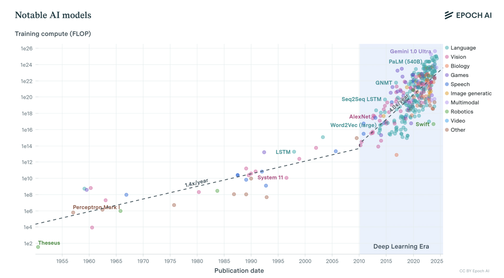
The semiconductor industry is undergoing a structural paradigm shift driven by the scale of generative AI demand. As ASML CEO Christophe Fouquet stated, frontier labs are no longer satisfied with traditional Moore's law timelines. Instead of waiting two years for a 2x increase in number of transistors, chip designers like NVIDIA are aiming to scale the entire system level performance 16x over the same timeframe, which is widely recognised as Huang's Law. This pace is not only driven by increasing transistor counts, but also by multi-chip packaging (linking multiple silicon die into a single system), massive capital expenditure and expanding gigawatt scale data infrastructure.
This aligns with Dario Amodei's perspective on AI progress. Amodei forecasts that as compute scaling moves up the exponential curve (shaped like a hockey stick), the rate of advancement almost appears vertical, wherein a single year's advancement today can deliver technological breakthroughs that historically took a decade to achieve.
The "AI supercycle" is a structural shift and capital is not shy of being invested in. The total semiconductor market is projected to reach $1.6T revenue in 2026, segmented by sector and chip architecture:
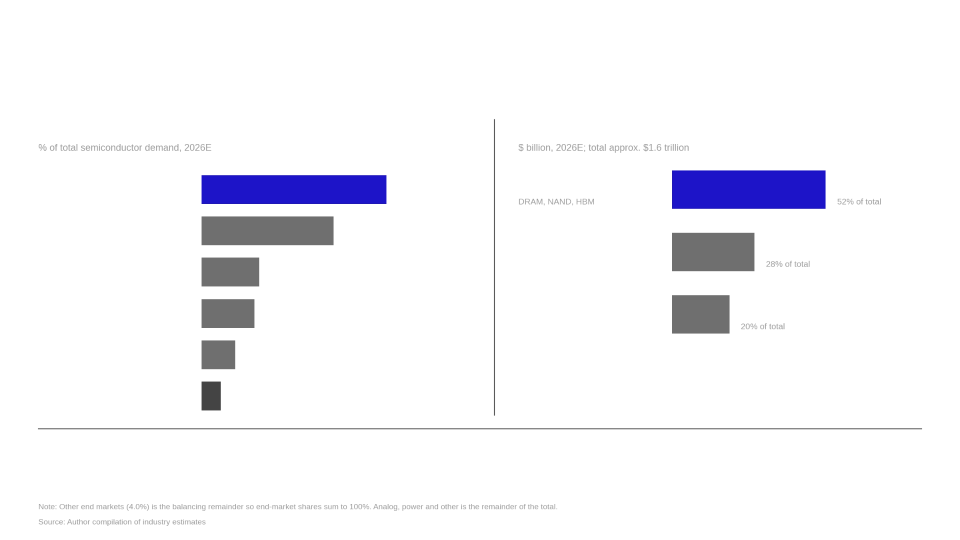
AI data centre infrastructure funded by hyperscalers and frontier labs comprise 36.5% to 55% followed by smartphones at 20% and lastly automotive and industrials taking up 12% and 15% respectively. Here, memory chips (DRAM, NAND, HBM) have a $837 Billion market value, followed by logic and microprocessors at $450 Billion and lastly analog and power chips at $313 Billion.
Demand is drastically outstripping physical supply capacity. The current demand to supply ratio for advanced AI chips is 13:1 and the supply chain is sold out until 2028. Although ASML plans to expand its factory capacity 30% annually, lithography supply will fall short of market demand through 2027 and 2028. For enterprises, this forces a shift from capital expenditure (buying physical hardware) to operational expenditure (renting compute from hyperscalers). Simultaneously, because chip manufacturers are chasing high margins of AI chips, they are reducing production for conventional chips. This capacity cannibalisation introduces "chipflation" across consumer electronics, automotive and industrial sectors. Ultimately, some of the rising costs will be absorbed by companies, but the rest will be passed down to end consumers to protect their margins.
Counterfactual Scenarios
Despite the shortage now, the the supply chain is very efficient. Rising demands, expansion of manufacturing spaces as a result, efficient distribution and customer satisfaction. It would be naive to assume that systems run unchanged forever. Two main risks matter:
Unhedgeable geopolitical disruption and export controls
The 2023 US restrictions on ASML equipment exports to China forced Beijing into a state backed innovation. China has invested billions into semiconductor funds to building an alternative and they are approaching it as a crisis, which tends to produce results. Its most credible pathway is a multi-beam maskless lithography, which imprints patterns with particle beam rather than light. This technology can print features far finer than EUV, but the West abandoned this approach since it collapsed throughput, with a single chip manufactured taking hours. China claims multi beam cuts this to minutes. But building a multi-beam system is one of the hardest engineering challenges in the world and demands immense capital. The physics works, but commercial viability is yet to be solved.
Technological disruption through a competitor
Elon Musk's newly introduced Terafab aims to be the largest vertically integrated semiconductor facility to produce orbital AI compute at unprecedented scale. IN near to middle terms, it has potential to be ASML's biggest customer and its projections are already factored into the ASML's 2027–2028 capacity expansion plans.
However, true disruption depends on how Musk could change the physics of chipmaking. Traditional EUV relies on laser produced plasma (LLP) to generate light. By contrast, free electron laser (FEL) technology is a centralised particle accelerator that replaces the light source LLP. If Terafab bankrolls or acquires xLight's FEL prototype (targeting 2028), and proves an industrial grade alternative, it would force ASML to adapt its scanners to accept external FEL light or transform Terafab from its biggest customer to its most credible long term rival. Yet, full vertical integration carried its own challenges. Nikon and Canon were more vertically integrated than ASML, and that is exactly why they fell behind in adopting EUV.
Bottom Line
Does the world need another ASML? No. The R&D flywheel, supplier lock in and customer co-optimisation raise barriers to entry to the sky. Geopolitical disruption aside, the most realistic threat would not be another lithography technology company but a fully vertically integrated buyer that decides the bottleneck is worth internalising. Whether that happens is worth watching.